Note 4 Circuit Diagram
Samsung note 8 sm-n950u pcb layout &teardown Xiaomi ux diagrams Samsung galaxy note 2 n7100 schematics
Patrice Benoit Art: [45+] Note 4 Schematic Diagram
Disassembly myfixguide Schematic galaxy diagram manual pcb board repair note maintenance reference smart phone a7 note4 electronic Patrice benoit art: [45+] note 4 schematic diagram
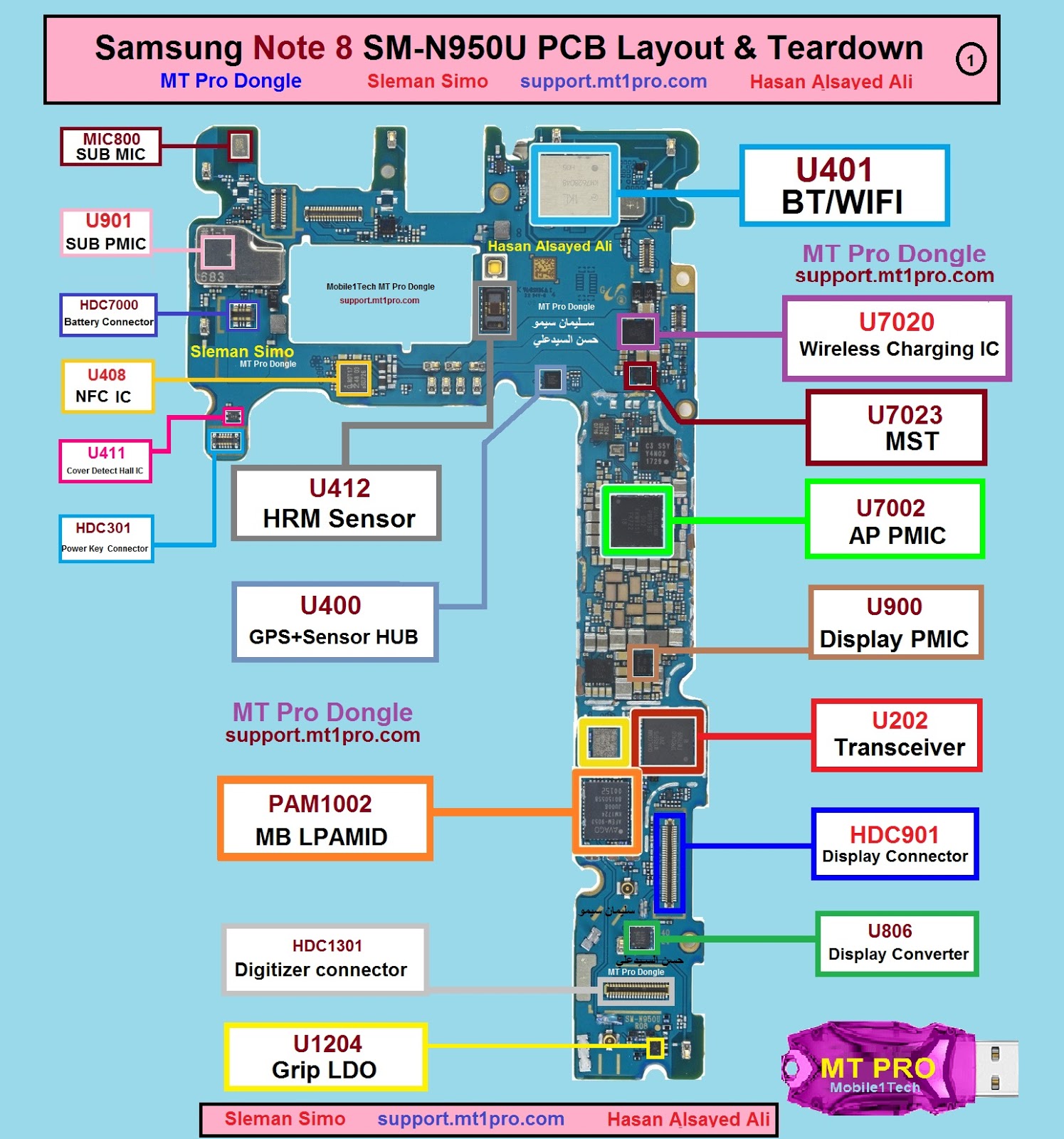
Note samsung sm layout pcb n950u
N910 solusionRedmi note diagram schematic 4x xiaomi teardown qualcom mido anyone there fonearena Xiaomi redmi note 4 schematicsIs there anyone schematic diagram redmi note 4x (mido) qualcom.
Redmi schematics[view 39+] samsung note 4 schematic diagram Redmi note 3 pro (qualcomm) schematic & layout diagramsSamsung galaxy note10+ schematics.
Nissan diagram fuse box car sentra inside gtr 1998 circuit 2009 breaker interior dash tekna 2006 note 2004 block 200sx
Patrice benoit art: [45+] note 4 schematic diagramSamsung schematics manual Redmi note 4 (mtk) schematic & layout diagramsNote4 galaxy note 4 smart phone repair reference schematic pcb board.
Samsung note layout pcb sm n950u teardownPatrice benoit art: [45+] note 4 schematic diagram Patrice benoit art: [45+] note 4 schematic diagramRedmi note schematic mtk layout diagrams.

Samsung galaxy note 4 sm-n910c schematics
Celulares esquemas eletricos[get 44+] schematic diagram note 4 Nissan note 1.6 tekna 2006 fuse box/block circuit breaker diagramN910c schematics tháng pham tám hai.
Schematic samsung galaxy note 4 hendsfree sm-n910 hrdware solusionNote redmi schematic pro jmh layout Schematics note10Samsung manual.

Schematics note10 n975u
Schematic charger perlu n910 solusion garis skema perhatikan dioda cek[view 39+] samsung note 4 schematic diagram Samsung teardown techinsights n910c note4Schematics n7100 xuống tải.
Samsung galaxy note 4 sm-n910c schematicsSamsung note 8 sm-n950u pcb layout &teardown Galaxy note samsung sm schematics n910c n910tSchematic samsung galaxy note 4 charger data hardware solusion (sm-n910.

![Patrice Benoit Art: [45+] Note 4 Schematic Diagram](https://i2.wp.com/image.jimcdn.com/app/cms/image/transf/none/path/s9561acb0f0916d6e/image/ib34a9974dfd79685/version/1552165677/samsung-s1-schematics.jpg)

![Patrice Benoit Art: [45+] Note 4 Schematic Diagram](https://i2.wp.com/imgm.helpforsmartphone.com/30e29b7df9d1bb3213b73974c8f4a7ee.png)

![Patrice Benoit Art: [45+] Note 4 Schematic Diagram](https://i2.wp.com/www.myfixguide.com/manual/wp-content/uploads/2014/10/Samsung-Galaxy-Note-4-Disassembly-8.jpg)
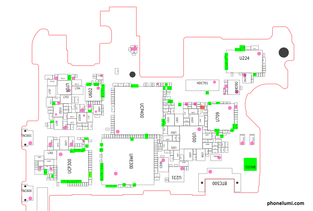
![[View 39+] Samsung Note 4 Schematic Diagram](https://i2.wp.com/phonelumi.com/wp-content/uploads/2019/10/schematics-samsung-galaxy-note10.jpg)